
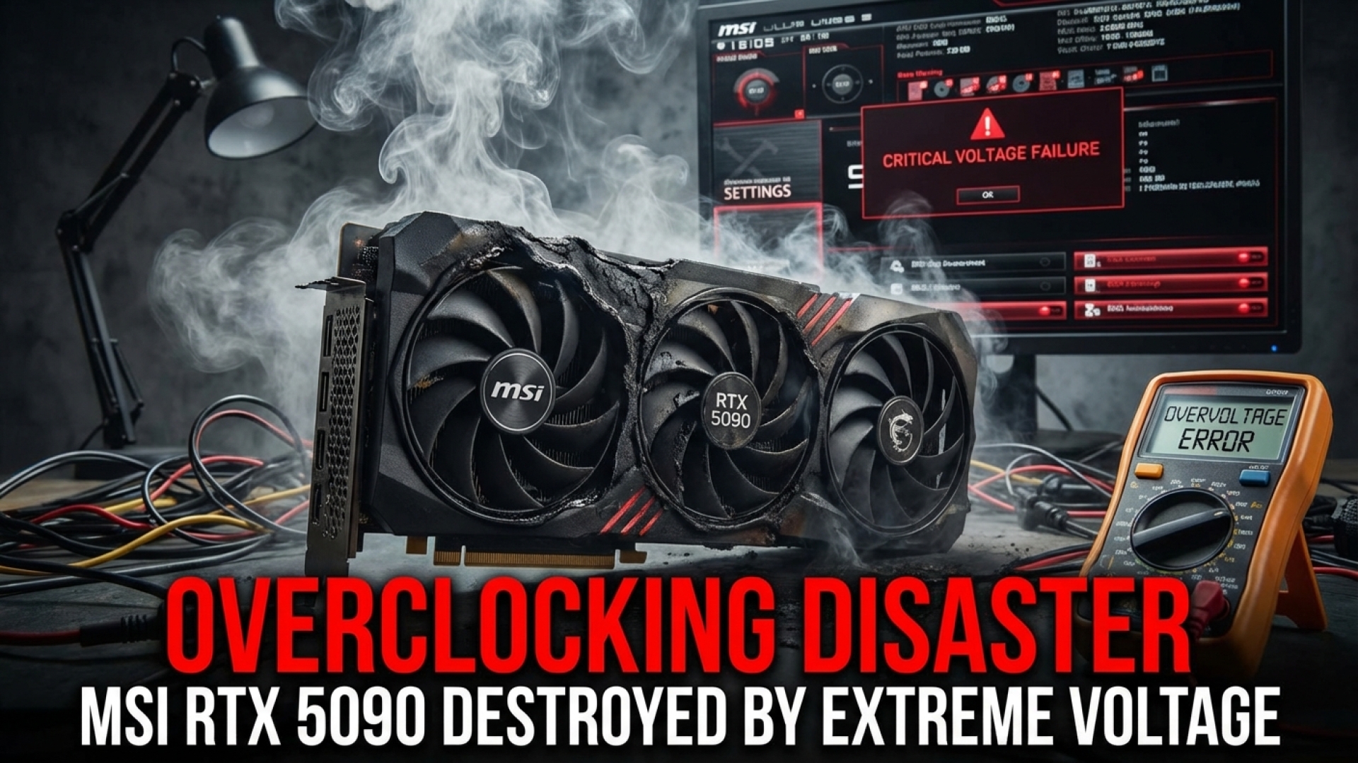
The world of extreme hardware overclocking is a high-stakes game where silicon is the currency and liquid nitrogen is the lifeblood. Here at Digital Tech Explorer, we love a good tale of engineering pushed to its absolute limits, but even the most robust hardware has a breaking point. Today’s story involves the legendary overclocker Alva Jonathan (aka Lucky_n00b) and a $5,000 piece of tech that met a spectacular, albeit tragic, end.
The centerpiece of this narrative is MSI’s new RTX 5090 Lightning Z. This isn’t your standard GPU; it’s a monster designed for those who find “standard” performance offensive. Boasting two 600 W 12V-2×6 connectors and 40-phase VRMs, it’s built to consume power like a small village. However, even with all that engineering, a single setting in a specialized BIOS turned this flagship into a $5,000 paperweight.
The Power of the Lightning Z: Breaking Down the Specs
In his recent deep dive, Alva Jonathan showcased early samples provided by MSI. While a reference GeForce RTX 5090 carries a hefty power limit of 575 W, the Lightning Z is designed to laugh at such restrictions. MSI has equipped this card with multiple “stages” of performance that cater to different levels of cooling solutions.
| Mode | Power Limit (W) | Recommended Cooling |
|---|---|---|
| Standard/Retail | 575 W | Stock Water Cooling |
| OC Mode | 800 W | High-End Custom Loop |
| Extreme Mode | 1,000 W | Chilled Water / LN2 |
| XOC (Extreme Overclocking) | 2,500 W | Liquid Nitrogen (LN2) ONLY |
As a software engineer and tech storyteller, I find the 2,500 W limit particularly fascinating. It’s a theoretical ceiling meant only for those chasing world records under sub-zero conditions. Unfortunately, physics has a way of asserting itself when the temperature doesn’t match the voltage.

A Tale of Thermal Shock and Cracked Silicon
The initial testing phase was a triumph. Jonathan managed to top the HWBot charts, securing a Geekbench 5 GPU Compute score of 683,433. It was a testament to what the RTX 5090 architecture can do when unshackled. But the quest for more performance led the team to engage the 2,500 W XOC BIOS.
This BIOS is a different beast entirely. It defaults to a voltage of 1.2 volts—a figure that seems small on paper but is catastrophic for a chip at ambient temperatures. Without the stabilizing cold of liquid nitrogen to manage the current density, the GPU die experienced what we call “thermal shock.”
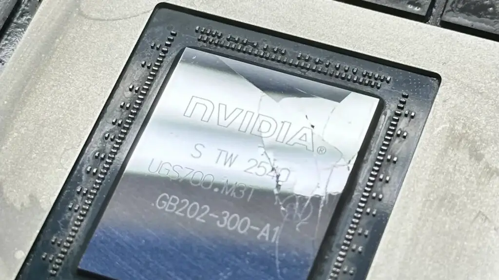
As Jonathan explained, that 1.2V level causes rapid current spikes. Silicon is remarkably brittle, and when certain sections of the die expand faster than others due to instantaneous heat, the material simply gives up. The result? The GPU die literally cracked apart as if it had been struck by a hammer, killing the card instantly upon startup.
Lessons from the Bleeding Edge
At Digital Tech Explorer, we emphasize transparency and real-world testing. While your average gaming rig will never see these voltages, this failure serves as a stark reminder of the delicate balance between software instructions (BIOS) and physical hardware limitations.
Jonathan wasn’t overly distraught—this is the nature of professional overclocking, and MSI had provided multiple samples for this exact reason. For the rest of us, it’s a fascinating look into the “X-factor” of hardware design. It proves that no matter how many VRMs or power connectors you add, the silicon itself remains the ultimate bottleneck.
Is there a practical takeaway for the everyday builder? Perhaps just this: always respect the BIOS. Even in a card designed for “lightning,” too much juice at the wrong time will lead to a very expensive thunderclap. For more stories on digital innovation and deep-dive hardware analysis, stay tuned to TechTalesLeo right here on Digital Tech Explorer.