
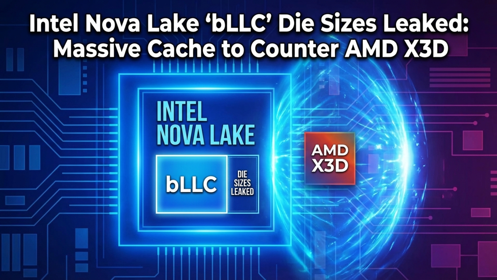
At Digital Tech Explorer, we love a good industry rivalry, and the latest chapter in the silicon wars is shaping up to be a classic. Recent leaks surrounding Intel’s Nova Lake CPUs are stirring the pot, particularly with the reveal of a high-cache variant. This “bLLC” version is designed specifically to challenge AMD’s dominance in the gaming sphere, currently held by the powerhouse Ryzen 7 9800X3D. As we dig into these architectural shifts, it’s clear that Intel is moving beyond incremental updates to rethink how cache memory influences hardware performance.
The “bLLC” Innovation: Intel’s New Strategy
The term “bLLC” stands for “big last level cache,” and it represents a strategic pivot for Intel. While AMD has found massive success with its 3D V-cache—a method of stacking a separate cache layer on top of the CPU—Intel is reportedly taking a more integrated approach. For the Nova Lake generation, this massive cache is expected to be built directly into the die itself. This structural difference could offer lower latency and improved efficiency across diverse workloads, potentially giving Intel an edge in more than just PC games.
Die Size and Architecture Breakdown
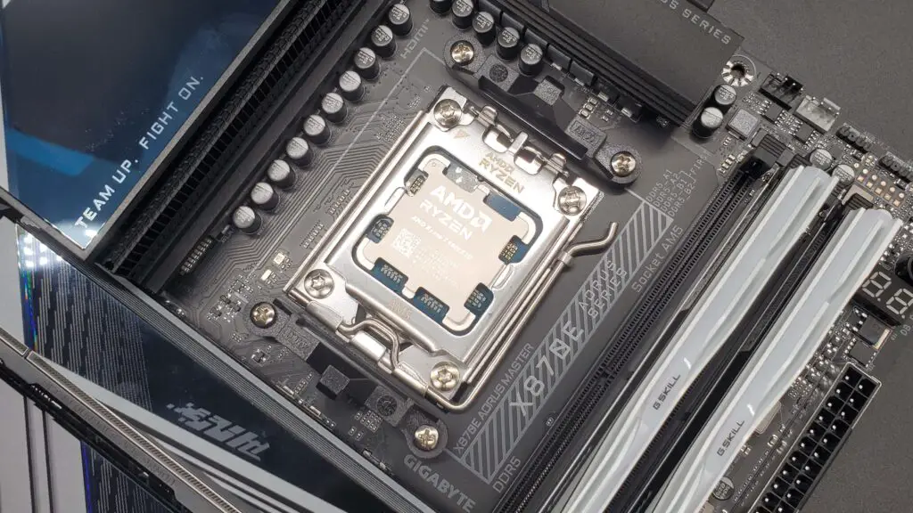
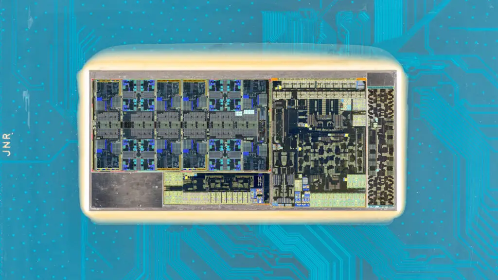
Integrating such a large cache comes with a physical cost: die real estate. Leaked data indicates that the standard Nova Lake die will measure roughly 110 mm², but the bLLC variant expands that footprint to approximately 150 mm². In comparison, the AMD Zen 5 die is a lean 71 mm². However, the “bigger is better” philosophy here accounts for a more complex core configuration; Intel is packing eight Performance (P) cores and 16 Efficient (E) cores into these chips, whereas the Zen 5 die focuses on eight high-performance standard cores.
| Processor Feature | Intel Nova Lake (Standard) | Intel Nova Lake (bLLC) | AMD Zen 5 (9800X3D) |
|---|---|---|---|
| Estimated Die Size | 110 mm² | 150 mm² | 71 mm² |
| Core Configuration | 8P + 16E | 8P + 16E | 8 Cores |
| Manufacturing Node | TSMC N2 / Intel 18A | TSMC N2 | TSMC N4 |
| Cache Highlight | Standard LLC | 144MB bLLC | 96MB Total (L3+V-Cache) |
Manufacturing: A Tale of Two Foundries
Intel’s manufacturing strategy for Nova Lake is as interesting as the architecture itself. Both die variants are expected to utilize TSMC’s N2 silicon node, a significant jump ahead of the N4 node used for AMD’s current Zen 5 lineup. This move toward TSMC for high-end variants mirrors the approach seen in AI acceleration and specialized GPU production. By leveraging the density of TSMC N2, Intel can cram more transistors into that 150 mm² space, while potentially utilizing its own 18A node for smaller, high-volume variants.
Cache Capacity and the Competitive Landscape
The headline-grabbing figure for the bLLC variant is the 144 MB of cache. When you compare that to the 96 MB of total L3 cache (including the 64 MB V-cache slice) found on the Ryzen 9800X3D, Intel is clearly aiming for a knockout blow in memory-intensive tasks. However, the tech world never stands still. By the time Nova Lake hits the shelves, AMD is expected to be ready with Zen 6, which will likely feature its own upgraded V-cache technology. This creates a fascinating dynamic for enthusiasts who prioritize frame rates and processing speed.
Release Timeline: When to Expect Nova Lake
While standard Nova Lake models are anticipated for a 2025/2026 rollout, it remains to be seen if the enthusiast-grade bLLC chips will debut simultaneously or follow as a mid-cycle “gaming king” refresh. If Intel follows the historical pattern of specialized chips, these cache-heavy models will be the primary focus for those building high-end gaming rigs. At Digital Tech Explorer, we’ll be tracking these developments closely to see if Intel can finally reclaim the gaming crown from AMD’s X3D series.
For more deep dives into the latest 2024 releases and beyond, stay tuned to our hardware section. This article was crafted by TechTalesLeo, bringing you the stories behind the silicon.