
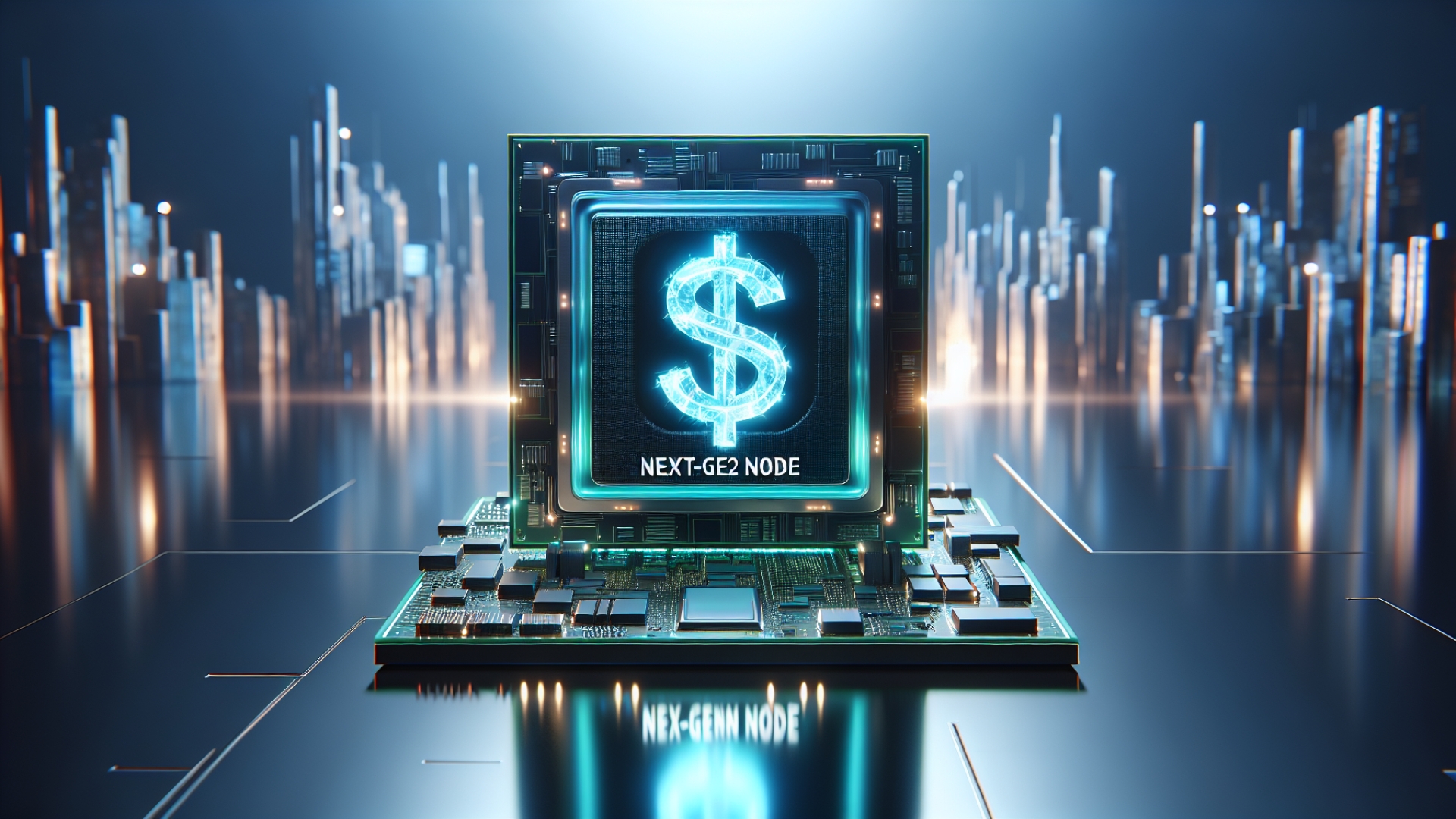
The relentless pursuit of technological advancement in high-end processor manufacturing comes at an ever-steepening cost. With each groundbreaking leap, the immense investments in advanced facilities, specialized machinery, and years of intensive research and development now stretch into the tens of billions of dollars. A recent, highly anticipated report indicates that TSMC, the world’s leading chip foundry, is poised to significantly escalate pricing for its upcoming N2 process node. This move could compel chipmakers to pass on these substantially higher manufacturing expenses, ultimately impacting the cost of our most crucial tech – from the latest smartphones to powerful AI GPUs and gaming PCs.
As detailed by a report from China Times, industry sources reveal that the price tag for TSMC’s cutting-edge N2 process node is projected to be over 50% higher than its N3 node. To put this into perspective for our tech-savvy readers at Digital Tech Explorer, the Taiwanese firm’s current leading node, N3P, already commands a premium, being approximately 20% more expensive than the preceding N5 generation.
Understanding the Escalating Costs of Semiconductor Manufacturing
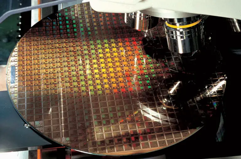
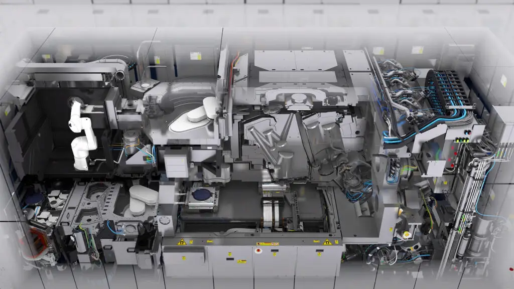
The continuous price hikes in semiconductor wafer manufacturing are, in many ways, an inevitable consequence of pushing the boundaries of technological advancement. Each new process node demands equipment far more sophisticated and precise than its predecessors. A prime example is the extreme ultraviolet (EUV) photolithography machines from Dutch giant ASML, which can cost a staggering $400 million per unit. While TSMC judiciously selects its tools and doesn’t yet deploy ASML’s newest high-NA EUV system for N2, the company consistently funnels billions annually into intensive research, development, and the construction of state-of-the-art fabrication plants—all prerequisites for these advanced process nodes. This continuous cycle of investment inherently drives up costs.
Further solidifying its pricing power, TSMC commands a dominant position in the global market. As the primary manufacturer for the world’s largest tech innovators, the foundry faces minimal direct competition in the bleeding-edge chip manufacturing arena. This formidable market presence grants TSMC considerable latitude to dictate its pricing, a factor directly influencing the entire tech supply chain.
Potential Financial Impact on Major Chipmakers
This compounding cost is stark: a 50% price jump for the N2 node, layered onto the 20% increase seen from N5 to N3, implies that major chipmakers such as Nvidia could face an eye-watering 80% higher cost per wafer compared to the N5 generation. Adding to the gravity of the situation, the China Times report indicates that N2 yields are already meeting required standards, suggesting TSMC has little immediate incentive to offer discounts or engage in significant price negotiations.
Indeed, TSMC’s most crucial clients—Apple, Nvidia, and AMD—are all reportedly lining up orders for N2 wafers, earmarking them for their next-generation phone chips, groundbreaking AI GPUs, and advanced processor chiplets. While it’s plausible these tech titans might secure some negotiated terms rather than pay the full advertised increase, one thing is unequivocally clear: any product leveraging the N2 node will fundamentally launch with a substantially elevated cost basis.
Customer Strategies: Passing Costs vs. Optimizing Die Size
This unprecedented situation presents a critical strategic dilemma for chip designers: will they simply pass this substantial price increase directly to consumers, or will they strategically absorb some of the cost by optimizing their chip designs? From TechTalesLeo’s perspective, one of the most effective strategies to mitigate rising wafer costs centers on utilizing smaller chip dies. This approach allows for a greater number of processors to be yielded from a single wafer, consequently reducing the overall wafer count required to satisfy market demand.
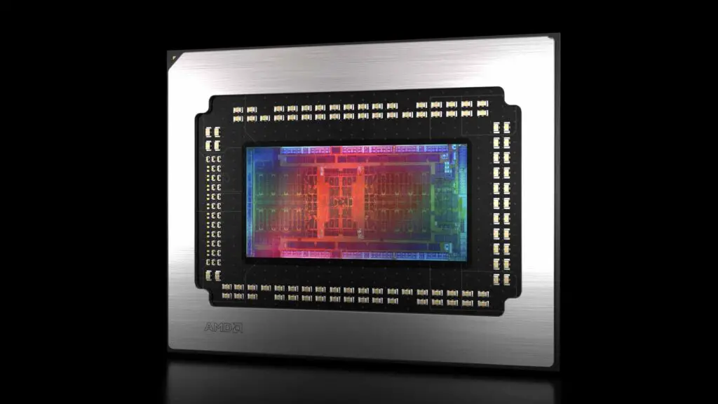
Crucially, a smaller chip die does not inherently equate to weaker performance. On the contrary, advancements in process nodes like N2 enable manufacturers to pack an even greater density of transistors into the same silicon footprint, often allowing for significantly higher clock speeds and improved power efficiency. A compelling illustration of this is the Navi 48 GPU within AMD’s Radeon RX 9070 XT, which demonstrates vastly superior performance compared to the Navi 21 found in the Radeon RX 6900 XT, despite being 31% smaller in physical size. This highlights the ongoing innovation Digital Tech Explorer loves to cover.
It’s a safe bet that Apple, Nvidia, and AMD will likely pursue a balanced strategy, navigating the middle ground between fully passing on the inflated costs and exclusively shrinking their processor dies. From our expert analysis here at Digital Tech Explorer, it wouldn’t be surprising to see the next generation of iPhone, GeForce, Ryzen, and Radeon chips offering only marginal performance improvements—perhaps in the realm of 10%—while simultaneously hitting consumers with a significant price increase, potentially around 30%, rather than the full, staggering 80%.
Even a more modest 30% price hike on popular PC processors and graphics cards will undoubtedly be a substantial hit to consumers’ wallets. To illustrate, a graphics card currently retailing for $300 could easily see its price tag surge to nearly $400, reshaping purchasing decisions for many tech enthusiasts.
As we look ahead, mass production of chips leveraging the N2 node isn’t anticipated until next year. Current predictions suggest AMD will likely be the first to introduce consumer-facing products built on this node, while Nvidia is expected to initially prioritize N2 for its high-demand AI GPUs. Therefore, for developers and gaming enthusiasts keen on understanding the real-world implications, the launch of the next generation of Ryzen processors will stand as the clearest, most tangible indicator of just how significantly TSMC’s N2 process node impacts the final cost for the end user. Digital Tech Explorer will be closely monitoring these developments, helping you stay ahead of the curve.