
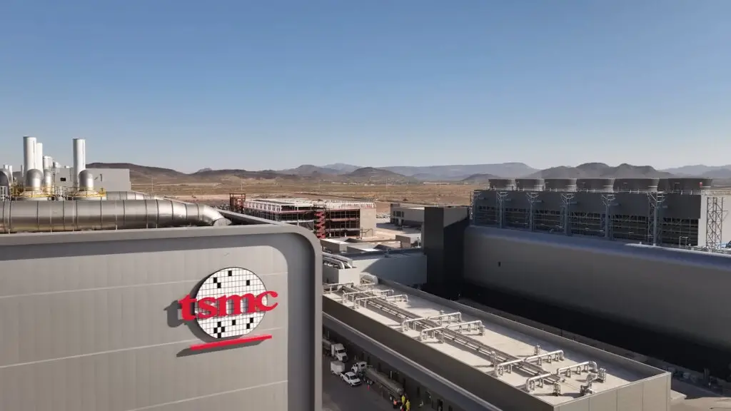
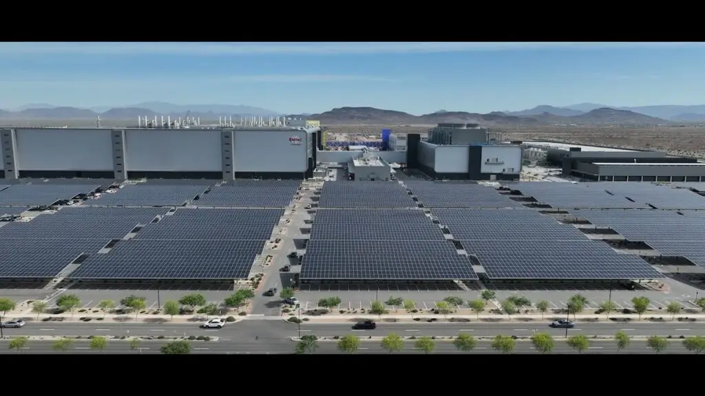
The future of advanced chip manufacturing in the U.S. is taking monumental shape as TSMC offers a captivating glimpse into its colossal new facility, TSMC Arizona. Nestled in the desert landscape just outside Phoenix, this site is more than a factory; it’s portrayed as a sprawling, city-like structure, a testament to the immense engineering and human effort invested. Through a promotional video, we see its vast, solar-panel-fronted exterior and interiors so futuristic they evoke the awe of “2001: A Space Odyssey.”
Forging the Future of US Chip Manufacturing
At the heart of TSMC Arizona’s mission is the aspiration to produce the world’s most advanced chips right here on US soil. This ambitious undertaking, as described by Rose Castanares, President of TSMC Arizona, is powered by a diverse and globally-sourced team. “On site we have 3,000 engineers, technicians, support folks, people from all over the US, from South America, from Asia. So many people coming together for a particular mission,” Castanares explains. This sentiment is powerfully echoed by TSMC Arizona vice president Y.H. Wu, who hailed the arrival of the first manufacturing machines as a “remarkable milestone” and emphasized their goal: “We bring [chip] manufacturing back to the USA.” This Arizona facility is part of a significant $65 billion investment specifically for the site, contributing to a broader $100 billion investment package in American manufacturing that includes plans for three additional fabrication plants, two advanced packaging facilities, and a new development center.
Inside the State-of-the-Art Fabrication Realm
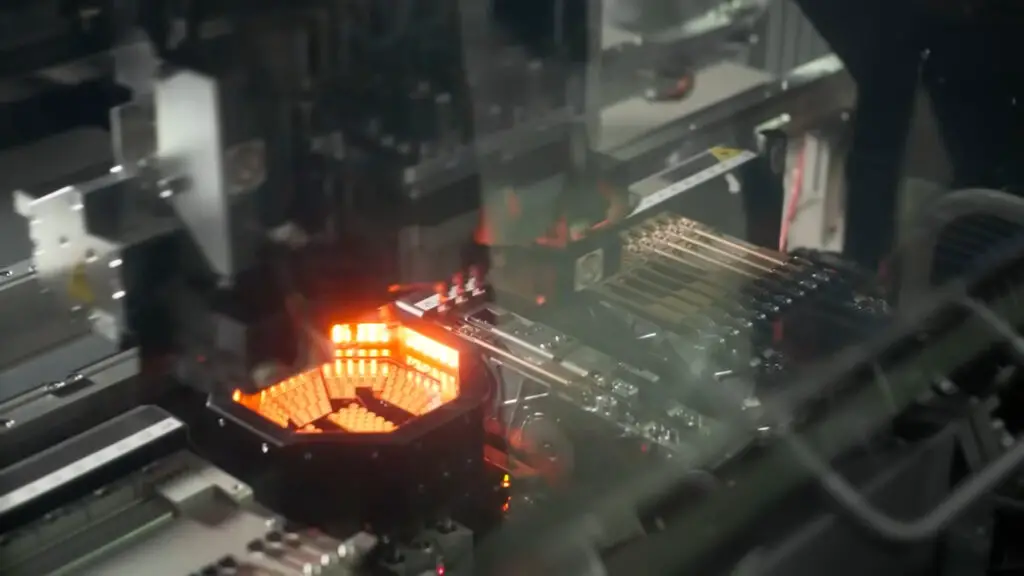
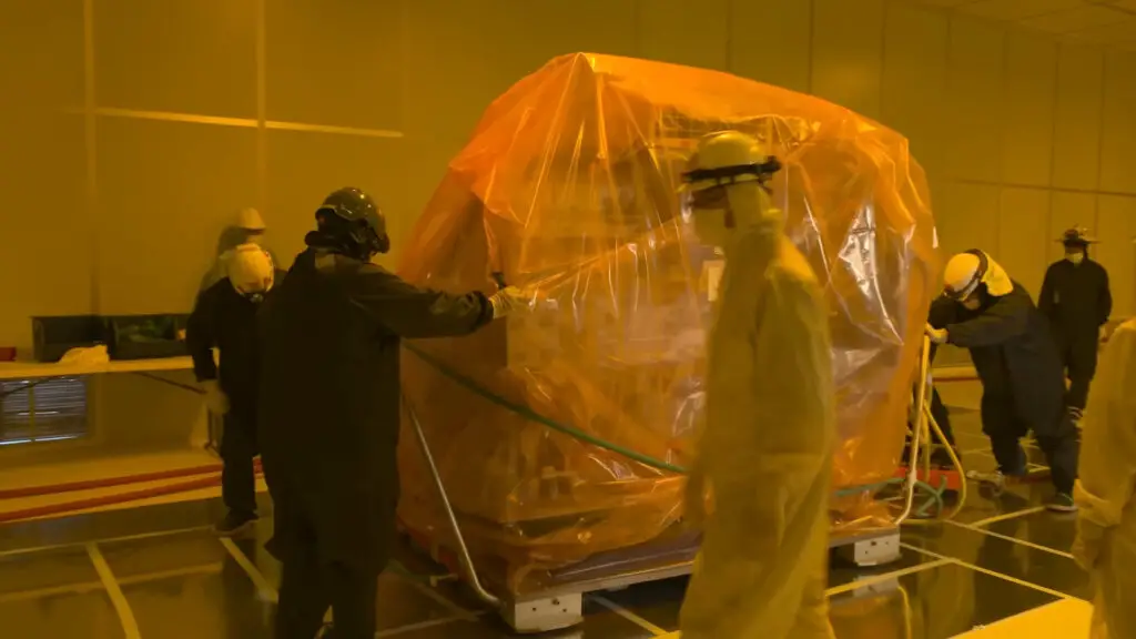
Stepping inside, the facility truly lives up to its “2001: A Space Odyssey” comparison, evoking the awe of a science fiction epic. Within its towering, yellow-lit clean rooms, hundreds of technicians in “bunny suits” navigate an environment meticulously designed to prevent even the slightest contamination. A key marvel is the Automated Material Handling System, affectionately nicknamed “the silver highway,” where robotic modules gracefully travel on ceiling-mounted rails, efficiently ferrying delicate wafers throughout the expansive plant. The intricate process also highlights the arrival of vital, advanced lithography equipment, the backbone of modern chip production.
Department manager Konstantinos Ninios articulates the sheer complexity: “In each one of these machines, there is a lot of high-tech going on. Plasma ignites. Molecules and atoms move around… one transistor is 10 to 20 thousand times smaller than a human hair.” This incredible precision and technological prowess are what enable the production of billions of transistors on a single chip – the minuscule yet mighty components that power everything from our smartphones to high-performance gaming PCs.
Navigating Environmental Responsibility and Water Management
A crucial consideration for any operation of this scale in the arid Arizona desert is water management. As Chris Camacho, former president and CEO of the Greater Phoenix Economic Council, candidly states, “We think about water on a daily basis.” Acknowledging these significant environmental concerns and criticism from local environmental groups, TSMC is proactively implementing solutions. Program manager Lacey Suastegui highlights their commitment: “Our industrial reclamation water plant will enable us to recycle and reclaim 90% of the water we use here.” While the fab commendably began producing 4nm chips in January, the water plant is reportedly still under construction, underscoring the continuous effort to harmonize technological advancement with essential environmental responsibility.
As Digital Tech Explorer continues to track such pivotal developments, TSMC Arizona emerges not just as an impressive feat of engineering but as a vital cornerstone in the expansion of US-based advanced chipmaking. For a company responsible for producing over 90% of the world’s most advanced chips, this sprawling Arizona plant, alongside a smaller fab in Washington, marks a strategic diversification of its global manufacturing footprint. The sheer scale, technological prowess, and collaborative spirit showcased within this facility underscore the monumental achievement behind the microscopic components that power our increasingly interconnected digital world.