

At Digital Tech Explorer, we often explore the forces shaping the tech landscape. While the AI boom, industry profiteering, and potential tariffs grab headlines for rising semiconductor costs, our author TechTalesLeo sheds light on a less-discussed yet critical factor: the incredibly precise specialized mirrors within EUV lithography machines. These marvels of engineering, as detailed by Asianometry, are foundational to the advanced chip manufacturing employed by titans like ASML, TSMC (for its N4 and N3 processes), and Intel (for its Intel 7 and 4 nodes), all dependent on extreme ultra-violet (EUV) light at a 13.5 nm wavelength.

The Unfathomable Precision in EUV Lithography
Controlling and focusing the 13.5 nm EUV light onto silicon wafers is an incredibly demanding process, essential for etching intricate patterns on modern semiconductors. This necessitates EUV mirrors crafted with almost unimaginable accuracy. The entire optical system, comprising multiple mirrors (typically 10 mirrors leading to up to 12 reflections depending on the specific configuration), must maintain a collective precision within 260 picometers—that’s a mere 0.26 nanometers. To contextualize this, it’s slightly smaller than a water molecule, which measures 275 picometers. Consequently, each individual mirror requires a surface accuracy of, at worst, 53 picometers. Asianometry strikingly notes this is comparable to the atomic radius of hydrogen, the smallest atom known.
Mirror Manufacturing Part 1: Crafting the Substrate and Initial Polishing
The journey to create these ultra-precise mirrors commences with the formation of a substrate. This base material is then meticulously polished to the target geometry using conventional optical techniques. However, this initial stage alone doesn’t achieve the extraordinary accuracy required. Subsequently, a sophisticated process known as ion beam figuring is utilized. This technique bombards the substrate with high-energy particles to painstakingly shave off surface imperfections, ultimately achieving atomic-level flatness.
Mirror Manufacturing Part 2: Applying Nanocoatings for EUV Reflection
Once atomic-level flatness is achieved, the subsequent critical phase involves the application of specialized nanocoatings. Alternating layers of molybdenum and silicon, each only a few nanometers thick, are deposited onto the mirror’s surface via magnetron sputtering. This method involves firing ions at targets of molybdenum or silicon, causing atoms to eject from the targets and settle onto the substrate. Approximately 50 such alternating layers are essential to create the multi-layer constructive interference. This complex structure, exemplified by the impressive ASML Carl Zeiss mirrors, enables the mirrors to efficiently reflect EUV light, a cornerstone of EUV lithography machine functionality.
Generating EUV Light: Another Intricate Engineering Feat
Beyond the mirrors themselves, the generation of the 13.5 nm EUV light is another fascinating, almost mind-bending, aspect of EUV machines. This highly complex process, simplified, involves firing powerful lasers at minuscule droplets of molten tin. Each droplet is precisely struck by an initial laser pulse to flatten it, followed by a second, more intense pulse to vaporize it. It is at this precise moment of vaporization that the tin emits the crucial 13.5 nm wavelength EUV light, showcasing yet another layer of sophisticated engineering inherent in these advanced systems.
The High Cost of EUV Technology and Its Ripple Effect on GPU Prices
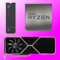
The painstaking manufacturing of EUV mirrors and the sheer complexity of EUV light generation significantly contribute to the staggering price tag of EUV lithography machines. A single ASML EUV machine can command a price of hundreds of millions of dollars, and the fabrication plants (fabs) built to house them represent multi-billion dollar investments. As Digital Tech Explorer aims to clarify for our readers, this enormous technological investment directly influences the cost of consumer electronics, most notably advanced GPUs. Industry leaders like TSMC utilize these expensive EUV systems, with their astonishingly accurate mirrors, to produce the latest GPUs for major brands, including the Nvidia RTX 50-series and AMD RX 9000-series. While not the exclusive factor, the immense expense of EUV technology and its hyper-specialized components, such as these mirrors, is a primary driver behind the escalating prices of modern graphics cards.
Related Hardware Buying Guides
- Best CPU for gaming: Top chips from Intel and AMD.
- Best gaming motherboard: The right boards.
- Best graphics card: Your perfect pixel-pusher awaits.
- Best SSD for gaming: Get into the game first.
Understanding the sophisticated technology behind EUV lithography, particularly the painstaking creation of its mirrors, offers a clearer picture of why cutting-edge processors and GPUs come with a significant price tag. Here at Digital Tech Explorer, in line with our mission, we believe that demystifying such complexities empowers tech enthusiasts and professionals alike. It allows for a deeper appreciation of the relentless innovation driving the digital world and helps in making more informed decisions. Stay tuned as TechTalesLeo continues to unravel the fascinating stories behind the technology that shapes our future.
All content on Digital Tech Explorer is for informational and entertainment purposes only. We do not provide financial or legal advice. Some of the links on Digital Tech Explorer are affiliate links. This means we may earn a commission if you click through and make a purchase, at no additional cost to you. Our recommendations are based on thorough research and personal experience.