
Since its highly anticipated release, the Nvidia DGX Spark mini AI box has sparked considerable debate within the tech community. While undeniably a marvel of engineering, its premium price tag and questions surrounding its real-world performance have left many seeking clarity. Now, a notable voice has joined the discussion: John Carmack, the legendary developer behind games like Doom, suggests this compact AI powerhouse is grappling with thermal limitations that significantly hinder its advertised capabilities. This insight prompts crucial considerations about the suitability of the chip at the DGX Spark’s core for potential integration into future laptop APUs, a topic of keen interest for us at Digital Tech Explorer.
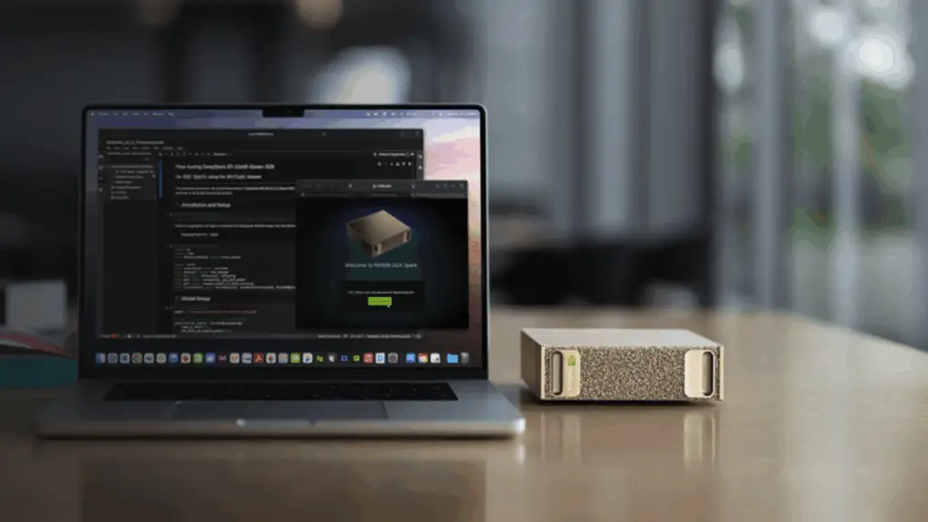
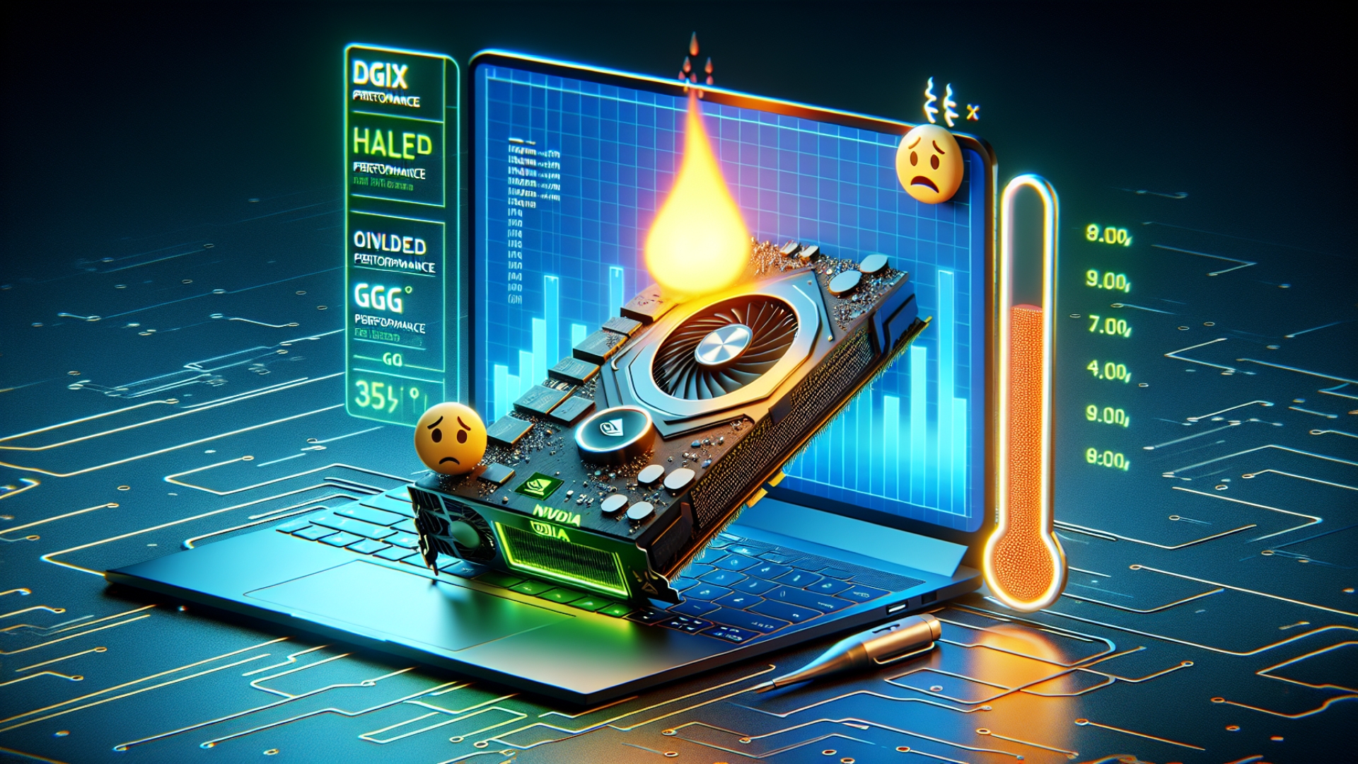
In a recent post on X (formerly Twitter), Carmack shared that his personal DGX Spark unit is only drawing approximately 100 watts of power. This is notably less than what he understood to be its rated 240 watts. This significant reduction in power draw, he observed, translates to roughly half of Nvidia’s quoted performance figures. Despite this apparent underperformance, Carmack noted that the device still runs quite hot. He also mentioned receiving reports of spontaneous reboots, which could indicate deeper underlying thermal challenges. These observations led him to speculate whether Nvidia might have “de-rated” the DGX Spark before its official release, a common practice to ensure stability when thermal envelopes are tight.
Unpacking the Power Ratings and Performance Claims
Nvidia has not been entirely forthcoming with the comprehensive specifications for the Nvidia DGX Spark. While Carmack initially cited a 240W rating for the box, official Nvidia documentation doesn’t explicitly state a precise power rating for the unit itself. Some industry discussions suggest that the 240W figure might have stemmed from an earlier, potentially erroneous, mention by an Nvidia representative. It’s also plausible that the 240W number refers to the capacity of the power supply unit for the DGX Spark, rather than the sustained power draw of the chip within.
Regarding performance, Carmack suggested that the DGX Spark appeared to deliver only about half of its quoted performance. He arrived at this conclusion by assuming an equivalence where 1 petaflop of sparse FP4 performance roughly translates to 125 teraflops of dense BF16 performance, effectively converting Nvidia’s headline 1 petaflop FP4 performance into the more commonly benchmarked BF16 metric. As TechTalesLeo often emphasizes, understanding these technical nuances is key to truly evaluating a product.
Deciphering FP4 and BF16 in AI Computing
To fully grasp Carmack’s performance conversion, it’s essential to understand FP4 and BF16. FP4, or floating-point four, refers to a low-precision compute standard that leverages only four bits of data. This format is prized for its ability to execute operations at incredibly high speeds, making it efficient for certain AI inference tasks. BF16, or Bfloat16, is another specialized numerical format, explicitly designed for deep learning and AI training. It offers the expansive numerical range of the full-precision FP32 format but with the significant benefits of reduced computational cost and a smaller memory footprint, balancing precision with efficiency.
One factor that could complicate Carmack’s direct performance conversion is Nvidia’s distinct approach to hardware design. The chip powering the DGX Spark, along with all of Nvidia’s GPUs based on the Blackwell architecture – including the upcoming RTX 50-series gaming GPUs like the RTX 5090 – incorporates dedicated hardware engineered specifically to accelerate FP4 performance. This specialized optimization means that a conventional equivalence often assumed between FP4 and BF16 performance might not directly apply in this context. However, given Carmack’s profound technical expertise, it’s highly probable his assessment considers these architectural nuances, making his observations even more compelling for tech enthusiasts and developers.
Regardless of the intricate performance metrics and power rating debates, it’s clear that the DGX Spark has not had an entirely smooth introduction. The thermal limitations highlighted by John Carmack cast a shadow of doubt on the broader applicability of the chip found within this mini AI box.
The chip, known as GB10 in the DGX Spark, is widely anticipated to be rebranded as N1 for other device applications, including potentially serving as a premium APU for laptop PCs. However, the reported thermal throttling within a compact desktop enclosure, such as the DGX Spark, does not bode well for its performance when integrated into a considerably slimmer laptop chassis. This is a critical point for developers and tech enthusiasts monitoring the mobile computing landscape.
It’s worth noting that the GB10 / N1 chip is manufactured on what is now considered a relatively mature TSMC N4 node. This manufacturing process, coupled with the chip’s inherent size and power requirements, naturally positions it as a significant power consumer in a mobile context, making thermal limitations less surprising. On the other hand, the DGX Spark chassis itself is ultra-compact, potentially even excessively so, which could severely restrict its thermal dissipation capabilities. Consequently, a laptop chassis might not necessarily present a much worse thermal environment, especially with dedicated cooling solutions. Ultimately, the performance of GB10 / N1 in future laptops, should a mobile variant ever be released, will undoubtedly be a compelling area of interest and thorough product review for Digital Tech Explorer.