

The world of computing is in a constant quest for enhanced speed and efficiency, especially concerning memory performance. Here at Digital Tech Explorer, we’re always on the lookout for innovations that help developers and tech enthusiasts stay ahead of the curve. In an exciting development for hardware, a recent AMD patent application has surfaced, revealing an ambitious new approach to DDR5 PC memory. Dubbed the High-Bandwidth Dual Inline Memory Module (HB-DIMM), this innovative design promises to significantly enhance memory bandwidth through clever implementation of pseudo channels, buffer chips, and advanced signal routing. While its technical potential is clear, its integration into mainstream PCs remains a captivating subject for our ongoing exploration of cutting-edge tech.
This intriguing discovery, initially brought to light by Tech4Gamers, keenly addresses a critical challenge in modern computing: the escalating demand for memory bandwidth. As high-performance graphics processors and multi-core servers become increasingly prevalent, the need for rapid data transfer rates is quickly outpacing the roadmap of improvements in traditional DDR DRAM chips. The official AMD patent application articulates this pressing issue, stating: “Because the memory bandwidth required for applications such as high-performance graphics processors and servers, which have multiple cores and a corresponding increase in bandwidth-per-core requirement, are outpacing the roadmap of bandwidth improvements for DDR DRAM chips, improved DIMM architectures are needed to meet such requirements with current DDR chip technologies such as DDR5.” AMD’s proposed solution, the HB-DIMM, aims to bridge this performance gap by bringing some advantages typically associated with High-Bandwidth Memory (HBM) into the more conventional DIMM form factor.
Technical Dive: Unpacking HB-DIMM Architecture
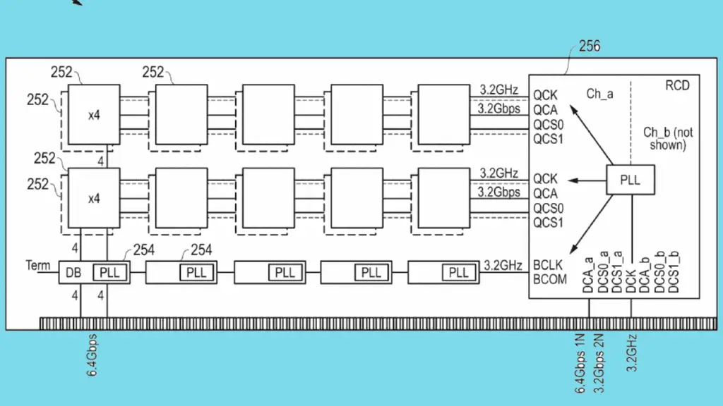
At the core of each HB-DIMM module lies a sophisticated combination of memory chips and buffer chips. As detailed in the patent, “The data buffer chips are coupled to respective sets of the memory chips and transmit data from the memory chips over a host bus at a data rate twice that of the memory chips.” This clever architecture further integrates “pseudo” memory channels and advanced signaling mechanisms. A central RCD (Registering Clock Driver) circuit plays a crucial role, featuring both a host bus interface and a memory interface connected to multiple memory chips. This circuit expertly processes commands received via the host bus, directing command/address (C/A) signals to the memory chips. The result is the creation of at least two independently addressable pseudo-channels, with each pseudo-channel being addressed based on a chip identifier (CID) bit derived from the C/A signals. This intricate design offers a glimpse into AMD’s commitment to pushing performance boundaries.
Essentially, this innovative system emulates a dual-channel memory interface within a single physical DIMM. The practical and impressive outcome is a potential doubling of the native 6.4 Gbps data rate of current DDR5 memory, pushing it to an astounding 12.8 Gbps. What makes this advancement particularly noteworthy for hardware enthusiasts and developers is that this significant performance boost is achieved using existing DDR5 memory chips, thereby eliminating the immediate need for an entirely new generation of silicon components. It’s a testament to ingenious engineering, extracting more from current technology.
The Road Ahead: Challenges for HB-DIMM Adoption
However, as with many pioneering digital innovations, the successful adoption of HB-DIMM faces considerable hurdles. Integrating this new standard would necessitate compatible CPUs, chipsets, and motherboards, a level of industry-wide alignment that is far from guaranteed. History teaches us that proprietary memory standards have often struggled to gain widespread traction in the broader PC market. The patent filing itself candidly acknowledges that “most DRAM chips sold today are compatible with various double data rate (DDR) DRAM standards promulgated by the Joint Electron Devices Engineering Council (JEDEC).” For the PC industry, adherence to these widely accepted JEDEC standards is typically a prerequisite for market dominance.
The crucial question, then, revolves around the likelihood of this intriguing new standard being embraced by the wider industry. One viable path for widespread adoption would be for JEDEC to incorporate it as an open standard, making it freely available for use across the ecosystem. It is highly improbable that Intel, a dominant force in PC platforms, would be willing to pay AMD for access to such fundamental memory technology. Therefore, Intel’s active support or the technology’s open standardization would likely be a prerequisite for HB-DIMM to become a truly viable and ubiquitous solution in the broader PC landscape. As Digital Tech Explorer, we’ll be closely monitoring how this unfolds, helping our readers make informed decisions about future hardware trends.
Through TechTalesLeo’s insightful analysis, we strive to bridge the gap between complex technology and everyday usability. The AMD HB-DIMM patent application represents a significant step in the ongoing evolution of memory technology, and its journey from concept to potential market reality is one we’ll continue to track with detailed updates and practical insights for our community of tech enthusiasts and professionals.